品牌 其他品牌 供货周期 一周
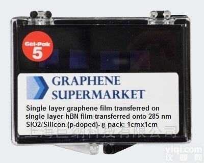
CVD Graphene/CVD Hexagonal Boron Nitride heterostructure on SiO2/Si wafer
Properties of Graphene/h-BN Film:
Single Layer Graphene Film on Single Layer h-BN Film transferred onto 285 nm (p-doped) SiO2/Si wafer
Size: 1cmx1cm; 8 pack
The thickness and quality of each film is controlled by Raman Spectroscopy
The coverage of this product is about 98%
The films are continuous, with minor holes and organic residues
High Crystalline Quality
The graphene film is premodominantly single layer (more than 95%) with occasional small multilayer islands (less than 5% bi-layers)
Sheet Resistance: 430-800 Ω/square

Properties of Silicon/Silicon Dioxide Wafers:
Oxide Thickness: 285 nm
Oxide Thickness: 285 nm
Color: Violet
Wafer thickness: 525 micron
Resistivity: 0.001-0.005 ohm-cm
Type/Dopant: P/Boron
Orientation: <100>
Front Surface: Polished
Back Surface: Etched


本产品信息由(上海巨纳科技有限公司)为您提供,内容包括(CVD石墨烯与CVD氮化硼异质结构(8片装))的品牌、型号、技术参数、详细介绍等;如果您想了解更多关于(CVD石墨烯与CVD氮化硼异质结构(8片装))的信息,请直接联系供应商,给供应商留言。若当前页面内容侵犯到您的权益,请及时告知我们,我们将马上修改或删除。